- 您现在的位置:买卖IC网 > Sheet目录2001 > ISL26712IRTZ (Intersil)IC ADC 12BIT SAR 1MSPS 8-TDFN
ISL26712, ISL26710, ISL26708
6
FN7999.3
September 5, 2012
GAIN Positive Gain Error
± REF input range
-2
±0.1
2-1
±0.1
1
-0.75
±0.04
0.75
LSB
Negative Gain Error
-2
±0.1
2-1
±0.1
1
-0.75
±0.04
0.75
LSB
ANALOG INPUT (Note 11)
|AIN| Full-Scale Input Span
2 x VREF
(AIN+) – (AIN–)
V
AIN+,
AIN–,
Absolute Input Voltage Range
AIN+
VCM = VREF
VCM±VREF/2
V
AIN–
VCM± VREF/2
V
ILEAK Input DC Leakage
Current
-1
1
-1
1
-1
1
A
CVIN Input Capacitance
Track/Hold mode
13/5
pF
REFERENCE INPUT
VREF VREF Input Voltage
Range
VDD = 3V (1% tolerance
for specified
performance)
2.0
V
VDD = 5V (1% tolerance
for specified
performance)
2.5
V
ILEAK DC Leakage Current
-1
1
-1
1
-1
1
A
CREF VREF Input Capacitance Track/Hold mode
21/18.5
pF
LOGIC INPUTS
VIH
Input High Voltage
2.4
V
VIL
Input Low Voltage
0.8
V
ILEAK Input Leakage Current
-1
1
-1
1
-1
1
A
CIN
Input Capacitance
10
pF
LOGIC OUTPUTS
VOH Output High Voltage
ISOURCE = 200A
VDD - 0.3
V
VOL Output Low Voltage
ISINK = 200A
0.4
V
IOZ
Floating-State Output
Current
-1
1
-1
1
-1
1
A
COUT Floating-State
Output Capacitance
10
pF
Output Coding
Two’s Complement
CONVERSION RATE
tCONV Conversion Time
FSCLK = 18MHz
888
ns
tACQ Acquisition Time
FSCLK = 18MHz
200
ns
Fmax Throughput Rate
1000
kSPS
POWER REQUIREMENTS
VDD Positive Supply Voltage
Range
2.73.6
2.7
3.6
V
4.75
5.25
4.75
5.25
4.75
5.25
V
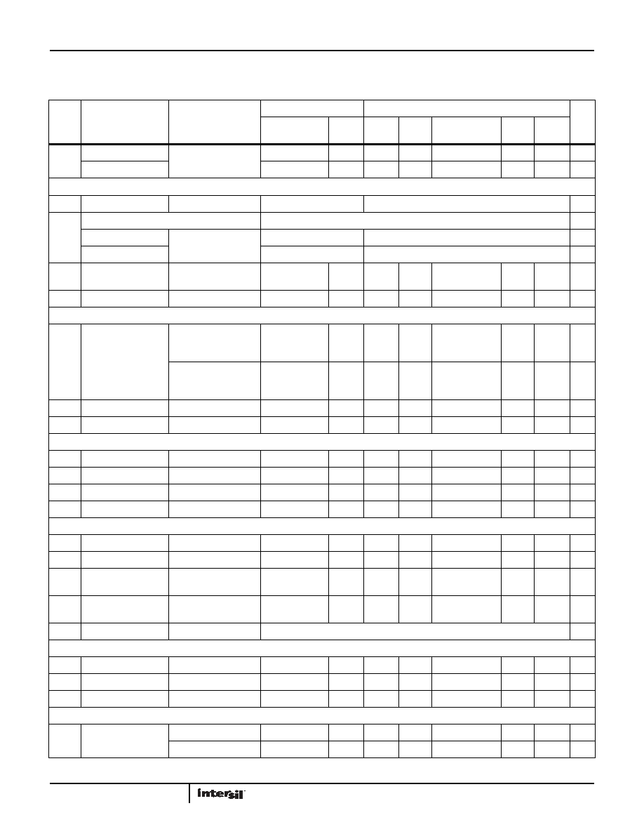
Electrical Specifications VDD = +3.0V to +3.6V, FSCLK = 18MHz, FS = 1MSPS, VREF = 2.0V; VDD = +4.75V to +5.25V, FSCLK = 18MHz,
FS =1MSPS, VREF = 2.5V; VCM = VREF, unless otherwise noted. Typical values are at TA = +25°C. Boldface limits apply over the operating temperature
range, -40°C to +85°C. (Continued)
SYMBOL
PARAMETER
TEST CONDITIONS
ISL26712
ISL26710
ISL26708
UNITS
MIN
(Note 10)
TYP
MAX
(Note 10)
MIN
(Note 10)
TYP
MAX
(Note 10)
MIN
(Note 10)
TYP
MAX
(Note 10)
发布紧急采购,3分钟左右您将得到回复。
相关PDF资料
ISL267450AIUZ
IC INTERFACE
ISL267817IUZ
IC INTERFACE
ISL32272EIVZ-T
IC TX RS422 QUAD 16TSSOP
ISL32273EIVZ
IC RCVR RS485/422 QD ESD 16TSSOP
ISL32470EIBZ-T7A
IC TXRX RS485 FAULT PROT 14SOIC
ISL32483EIBZ-T7A
IC TXRX RS485 FAULT PROT 14SOIC
ISL35822LPIK
IC CLOCK/DATA RECOVERY 192EBGA-B
ISL41334IRZ-T7A
IC TXRX RS232/485 DL 2PRT 40QFN
相关代理商/技术参数
ISL26712IRTZ-T
功能描述:IC ADC 12BIT SAR 1MSPS 8-TDFN RoHS:是 类别:集成电路 (IC) >> 数据采集 - 模数转换器 系列:- 产品培训模块:Lead (SnPb) Finish for COTS
Obsolescence Mitigation Program 标准包装:250 系列:- 位数:12 采样率(每秒):1.8M 数据接口:并联 转换器数目:1 功率耗散(最大):1.82W 电压电源:模拟和数字 工作温度:-40°C ~ 85°C 安装类型:表面贴装 封装/外壳:48-LQFP 供应商设备封装:48-LQFP(7x7) 包装:管件 输入数目和类型:2 个单端,单极
ISL26712IRTZ-T7A
功能描述:模数转换器 - ADC 12 BIT 1MSPS SAR ADC 8LD RoHS:否 制造商:Texas Instruments 通道数量:2 结构:Sigma-Delta 转换速率:125 SPs to 8 KSPs 分辨率:24 bit 输入类型:Differential 信噪比:107 dB 接口类型:SPI 工作电源电压:1.7 V to 3.6 V, 2.7 V to 5.25 V 最大工作温度:+ 85 C 安装风格:SMD/SMT 封装 / 箱体:VQFN-32
ISL267440
制造商:INTERSIL 制造商全称:Intersil Corporation 功能描述:10-Bit and 12-Bit, 1MSPS SAR ADCs
ISL267440IHZ-T
功能描述:IC ADC 10BIT SPI/SRL 8-SOT-23 RoHS:是 类别:集成电路 (IC) >> 数据采集 - 模数转换器 系列:- 产品培训模块:Lead (SnPb) Finish for COTS
Obsolescence Mitigation Program 标准包装:250 系列:- 位数:12 采样率(每秒):1.8M 数据接口:并联 转换器数目:1 功率耗散(最大):1.82W 电压电源:模拟和数字 工作温度:-40°C ~ 85°C 安装类型:表面贴装 封装/外壳:48-LQFP 供应商设备封装:48-LQFP(7x7) 包装:管件 输入数目和类型:2 个单端,单极
ISL267440IHZ-T7A
功能描述:IC ADC 10BIT SPI/SRL 1M 8SOT-23 RoHS:是 类别:集成电路 (IC) >> 数据采集 - 模数转换器 系列:- 产品培训模块:Lead (SnPb) Finish for COTS
Obsolescence Mitigation Program 标准包装:1 系列:- 位数:10 采样率(每秒):357k 数据接口:DSP,MICROWIRE?,QSPI?,串行,SPI? 转换器数目:1 功率耗散(最大):830µW 电压电源:单电源 工作温度:-40°C ~ 85°C 安装类型:表面贴装 封装/外壳:10-WFDFN 裸露焊盘 供应商设备封装:10-TDFN-EP(3x3) 包装:剪切带 (CT) 输入数目和类型:2 个单端,单极;2 个单端,双极;1 个差分,单极;1 个差分,双极 产品目录页面:1396 (CN2011-ZH PDF) 其它名称:MAX1395ETB+TCT
ISL267440IUZ
功能描述:模数转换器 - ADC 10 BIT 1MSPS SAR ADC 8LD 3 X 3 PROPRIETRY RoHS:否 制造商:Texas Instruments 通道数量:2 结构:Sigma-Delta 转换速率:125 SPs to 8 KSPs 分辨率:24 bit 输入类型:Differential 信噪比:107 dB 接口类型:SPI 工作电源电压:1.7 V to 3.6 V, 2.7 V to 5.25 V 最大工作温度:+ 85 C 安装风格:SMD/SMT 封装 / 箱体:VQFN-32
ISL267440IUZ-T
功能描述:模数转换器 - ADC 10 BIT 1MSPS SAR ADC 8LD 3 X 3 PROPRIETRY RoHS:否 制造商:Texas Instruments 通道数量:2 结构:Sigma-Delta 转换速率:125 SPs to 8 KSPs 分辨率:24 bit 输入类型:Differential 信噪比:107 dB 接口类型:SPI 工作电源电压:1.7 V to 3.6 V, 2.7 V to 5.25 V 最大工作温度:+ 85 C 安装风格:SMD/SMT 封装 / 箱体:VQFN-32
ISL267440IUZ-T7A
功能描述:模数转换器 - ADC 10 BIT 1MSPS SAR ADC IN 8LD RoHS:否 制造商:Texas Instruments 通道数量:2 结构:Sigma-Delta 转换速率:125 SPs to 8 KSPs 分辨率:24 bit 输入类型:Differential 信噪比:107 dB 接口类型:SPI 工作电源电压:1.7 V to 3.6 V, 2.7 V to 5.25 V 最大工作温度:+ 85 C 安装风格:SMD/SMT 封装 / 箱体:VQFN-32